How to make your own AVR Programmer?
1. Abstract
2. Introduction
3. Components
1. Crystal 12 MHz 1
= 0.2$
2. ZIF
40 1
= 1.5$
3. Capacitor 10uf 1
= 0.05$
4. Capacitor 15p *4, 104*2 6 = 0.2$
5. LED
red 1
= 0.025$
6. LED
blue 1
= 0.025$
7. USB
type B 1
= 0.3$
8. Male
connector line 1
= 0.3$
9. Resister
2.2k *1, 220 *4, 10k *1,1k*2 10 = 0.3$
10. Diode
Zener 3.6v 2 = 0.2$
11. IC Socket 1 = 0.3$
12. IC
Atmega8 1
= 3.0$
13. Acid 1 = 0.5$
14. PCB
Board 1 = 0.5$
Total = 7.7$
|
Pin No. |
Pin name |
Description |
Alternate Function |
|
1 |
PC6
(RESET) |
Pin6
of PORTC |
Pin by default is used
as RESET pin. If the RSTDISBL Fuse is programmed, PC6
can be used as an I/O pin. (Pulled HIGH to RESET
controller) |
|
2 |
PD0
(RXD) |
Pin0
of PORTD |
RXD (USART Input Pin) USART
Serial Communication Interface [Can be used for programming] |
|
3 |
PD1
(TXD) |
Pin1
of PORTD |
TXD (USART Output Pin) USART
Serial Communication Interface [Can be used for programming] INT2( External
Interrupt 2 Input) |
|
4 |
PD2
(INT0) |
Pin2
of PORTD |
External Interrupt INT0 |
|
5 |
PD3
(INT1) |
Pin3
of PORTD |
External Interrupt INT1 |
|
6 |
PD4 (XCK/T0) |
Pin4
of PORTD |
T0( Timer0 External
Counter Input) XCK ( USART External
Clock I/O) |
|
7 |
VCC |
VCC |
|
|
8 |
GND |
GOUND |
|
|
9 |
PB6
(XTAL1/TOSC1) |
Pin6
of PORTB |
XTAL1
(Chip Clock Oscillator pin 1 or External clock input) TOSC1
(Timer Oscillator pin 1) |
|
10 |
PB7 (XTAL2/TOSC2) |
Pin7
of PORTB |
XTAL2
(Chip Clock Oscillator pin 2) TOSC2
(Timer Oscillator pin 2) |
|
11 |
PD5
(T1) |
Pin5
of PORTD |
T1(Timer1
External Counter Input) |
|
12 |
PD6
(AIN0) |
Pin6
of PORTD |
AIN0(Analog
Comparator Positive I/P) |
|
13 |
PD7
(AIN1) |
Pin7
of PORTD |
AIN1(Analog
Comparator Negative I/P) |
|
14 |
PB0
(ICP1) |
Pin0
of PORTB |
ICP1(Timer/Counter1
Input Capture Pin) |
|
15 |
PB1
(OC1A) |
Pin1
of PORTB |
OC1A
(Timer/Counter1 Output Compare Match A Output) |
|
16 |
PB2
(SS/OC1B) |
Pin2
of PORTB |
SS (SPI
Slave Select Input). This pin is low when controller acts as slave. [Serial
Peripheral Interface (SPI) for programming] OC1B (Timer/Counter1 Output
Compare Match B Output) |
|
17 |
PB3
(MOSI/OC2) |
Pin3
of PORTB |
MOSI
(Master Output Slave Input). When controller acts as slave, The data is
received by this pin. [Serial Peripheral Interface (SPI) for programming] OC2
(Timer/Counter2 Output Compare Match Output) |
|
18 |
PB4
(MISO) |
Pin4
of PORTB |
MISO
(Master Input Slave Output). When controller acts as slave, the data is sent
to master by this controller through this pin. [Serial Peripheral Interface
(SPI) for programming] |
|
19 |
PB5
(SCK) |
Pin5
of PORTB |
SCK
(SPI Bus Serial Clock). This is the clock shared between this controller and
other system for accurate data transfer. [Serial Peripheral Interface (SPI)
for programming] |
|
20 |
AVCC |
VCC
for Internal ADC Converter |
|
|
21 |
AREF |
|
Analog
Reference Pin for ADC |
|
22 |
GND |
|
GROUND |
|
23 |
PC0
(ADC0) |
Pin0
of PORTC |
ADC0
(ADC Input Channel 0) |
|
24 |
PC1
(ADC1) |
Pin1
of PORTC |
ADC1
(ADC Input Channel 1) |
|
25 |
PC2
(ADC2) |
Pin2
of PORTC |
ADC2
(ADC Input Channel 2) |
|
26 |
PC3
(ADC3) |
Pin3
of PORTC |
ADC3
(ADC Input Channel 3) |
|
27 |
PC4
(ADC4/SDA) |
Pin4
of PORTC |
ADC4
(ADC Input Channel 4) SDA
(Two-wire Serial Bus Data Input/ Output Line) |
|
28 |
PC5
(ADC5/SCL) |
Pin5
of PORTC |
ADC5
(ADC Input Channel 5) SCL
(Two-wire Serial Bus Clock Line) |
4. Schematic, PCB layout and 3D view
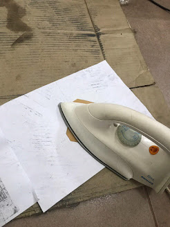
5. Process of PCB board
 |
 |
 |
 |
| 6) Finally, we need to insert all the component into the board |
 |
2) Solder all components on it, except the Mega 8. I suggest to solder a socket for it instead, so you can replace it later (in case of wrong programming the "Master" CPU")
3) Put your Mega8 (or 88/168/328) in the ZIF socket in the right position for Mega8. Put the RESET-Jumper P5 in the Position PROG.
4) Now stick another ISP Programmer (you only need to do this once) into the ISP header on the board and flash the USBasp-Bootloader on it.
5) Put the flashed Mega-8 in its socket and stick an Jumper on the SLOW Header P2 and connect the board to the PC.
6) The Mega8 will be now in a bootloader mode, where it simulates an USBasp which flashes its own MCU. Use this "bootloader-USBasp" to flash the real USBasp Firmware. Now disconnect the SLOW--Header and reconnect the USB.


0 Comments